Extraterrestrial Planet Discovery using Sensitive Light Detection Methods
In the realm of astronomy research, a team of design and electrical engineers embarked on an exciting project to create a Printed Circuit Board (PCB) for low photon detection transit photometry, with the primary goal of detecting extrasolar planets. The project utilized CadSoft EAGLE PCB Design software for design, and the programming language employed was C/C#.
The testing and debugging process for this sensitive PCB was a meticulous journey, involving several precise steps to ensure the board's electrical integrity, signal accuracy, and functional performance under real-world conditions.
1. Schematic Verification Before Fabrication
The process began with a detailed and well-structured PCB schematic to verify all electrical connections and component logic. A clear schematic helped identify design errors early and supported efficient debugging later.
2. Incorporate Test Points in PCB Design
The PCB was designed with strategically placed test points that allowed easy access to critical signals and power rails without interfering with the circuit or adding noise. This was crucial for sensitive photometry circuits to maintain high signal integrity and enable effective testing.
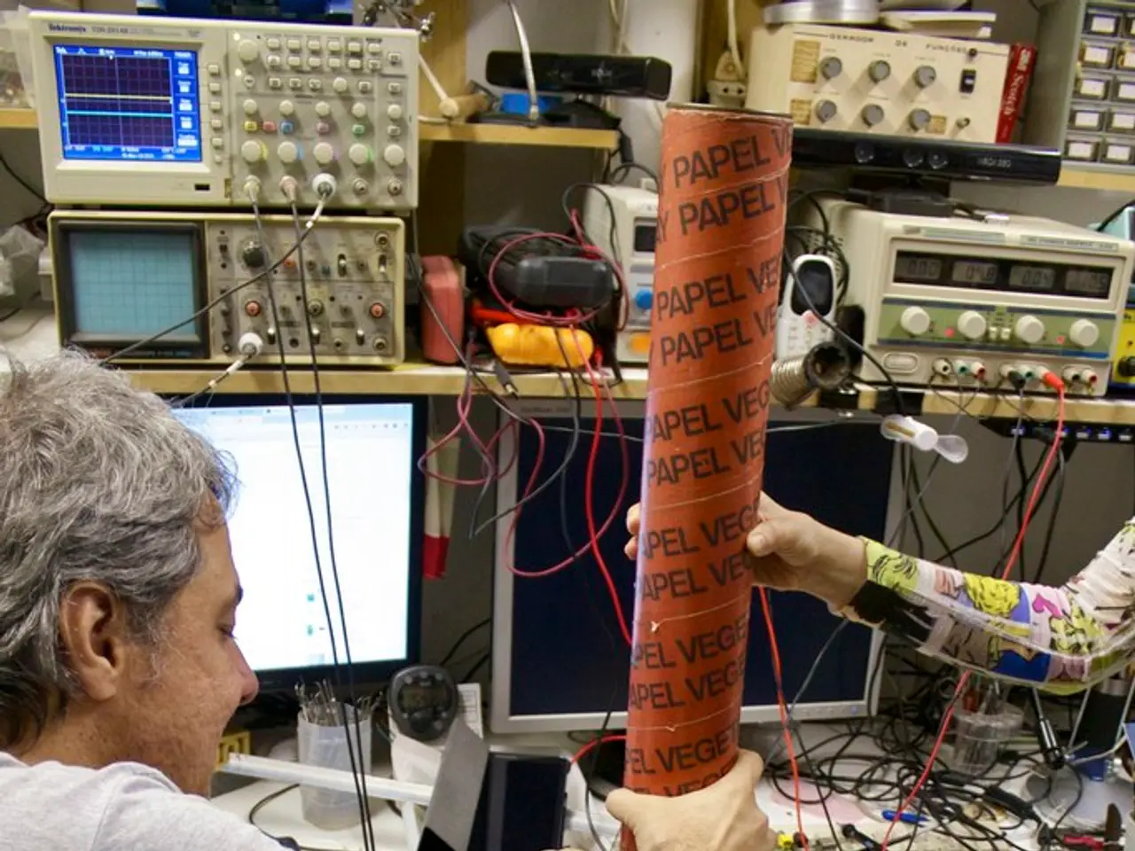
3. Electrical Testing: Continuity and Shorts
Using multimeters, the team manually checked continuity and the absence of shorts on critical nodes. This was fundamental since any shorts or open circuits would render the PCB unusable regardless of other aspects.
4. Functional Testing Under Simulated Conditions
The team powered up the PCB and applied test signals simulating the photon detection environment. They ran firmware or software controlling the detector to observe all inputs and outputs. Any malfunction or unexpected behavior was detected to pinpoint design flaws or assembly errors.
5. Use of Specialized Instruments
- Oscilloscopes were used to analyze signal integrity, timing, and noise, particularly important in low photon detection to distinguish real signals from background noise.
- Logic analyzers were employed if digital signals or communication protocols controlled sensor readouts and data acquisition.
6. Thermal and Noise Analysis
Due to the sensitivity of photon detection, thermal cameras were used to ensure components were not overheating, which could affect noise levels. Noise and interference susceptibility were minimized in layout and verified during testing.
7. Iterative Debugging with Documentation
Referring to schematic diagrams and test point documentation, the team localized faults efficiently when tests failed. They adjusted the design, firmware, or assembly accordingly, then repeated testing until specifications were met.
8. Leverage AI Tools if Available
Advanced debugging could be enhanced with AI-supported tools that analyzed component ratings, verified correct resistor and capacitor values, and helped visualize design weaknesses. Although not mandatory, such tools could reduce debugging time for complex boards in research settings.
The testing and debugging process was conducted in low-light conditions, reflecting the board's intended application. The project structure included the Pictavore Server, an ASCOM driver for Pictavore cameras, camera driver, filter wheel driver, focuser driver, and various .bat files.
In summary, testing and debugging such a sensitive PCB is a rigorous process combining electrical and functional verification, strategic test point access, signal integrity analysis, and iterative corrections guided by detailed schematics and documentation. This ensures the PCB performs reliably in low-photon astrophysical measurements needed for transit photometry.
Key instruments: multimeter, oscilloscope, logic analyzer, thermal camera. Key practices: schematic validation, test point planning, electrical continuity checks, functional simulation, noise and thermal evaluation, iterative debugging with documentation.
1. Utilizing Advanced Technologies for Verification
Given that the PCB design was executed with cutting-edge technology in mind, integrating AI-driven tools would have further optimized the schematic verification process, providing quicker identification of errors based on component ratings, standardized value checks, and potential design flaw visualization.
2. Space-and-Astronomy Application Underpinned by Science and Technology
This research venture transcends traditional engineering domains, merging science, space-and-astronomy, and technology to develop innovative solutions. The ultimate goal being the discovery and study of extrasolar planets with high-precision transit photometry, where advanced PCB designs play a pivotal role.

